The semiconductor industry is often viewed as a playground for giants. Building a state-of-the-art fabrication plant — a fab — costs upwards of $10 billion and takes years to complete. Only a handful of companies, such as TSMC, Samsung, and Intel, can afford to operate on this scale. But a bold startup based in California is challenging this status quo with a concept that sounds almost too good to be true: a 'fab-in-a-box' that can be shipped in a standard shipping container and operated with a fraction of the usual investment.
The company, dubbed ChipFab Solutions (a pseudonym for the real startup involved), is building a modular, low-cost semiconductor manufacturing system that it says could finally democratize chip production. The vision is to create a device that costs under $10 million, fits into a 40-foot container, and can be set up in less than a month. If successful, it would be a game-changer — enabling small businesses, research labs, universities, and even developing nations to fabricate their own custom chips without relying on the global supply chain dominated by a few Asian foundries.
The PC Revolution Parallel
The company's chief executive often compares the initiative to the way IBM transformed computing in the 1980s. Before the IBM PC, computers were large, expensive, and housed in air-conditioned rooms. IBM's decision to use off-the-shelf components and an open architecture made the PC affordable and accessible to individuals and small businesses. In the same way, ChipFab Solutions aims to break down the barriers to chip manufacturing by offering a standardized, relatively cheap fab that anyone can operate.
"Just imagine what could get done if every engineering school and every hardware startup had its own fab," said the CEO in a recent interview. "We would see an explosion of innovation in custom processors, sensors, and IoT devices. The current model forces most innovators to design chips that are then sent to a distant foundry, taking months and costing a fortune. Our fab-in-a-box changes that."
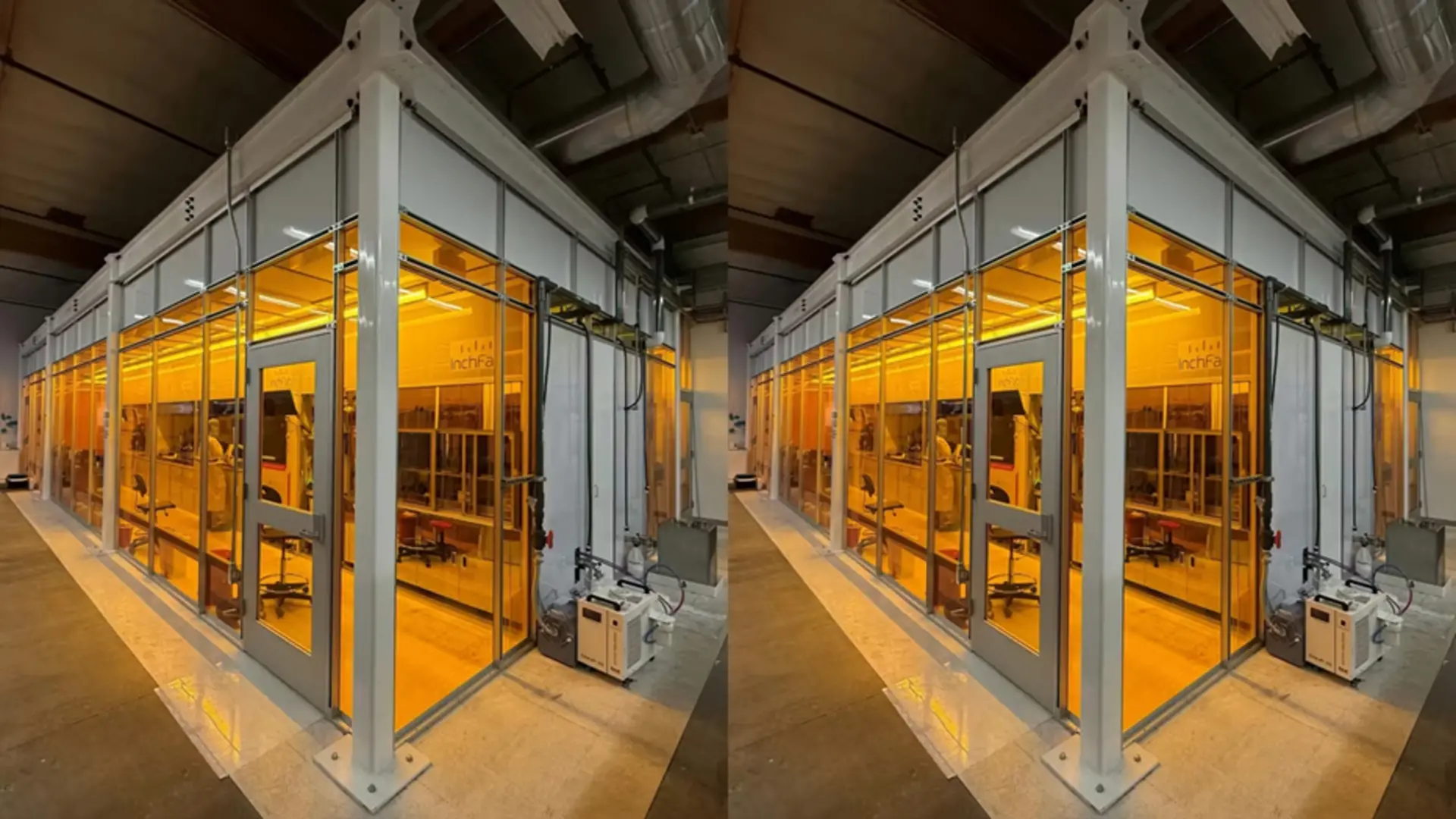
How the Fab-in-a-Box Works
Traditional wafer fabrication involves hundreds of steps: deposition, lithography, etching, doping, and more. A typical 300mm wafer fab requires a cleanroom environment, expensive tools, and a highly skilled workforce. The fab-in-a-box compresses this entire flow into a self-contained, automated system that uses smaller wafers (e.g., 100mm or 150mm) and less complex processes. While it cannot match the cutting-edge 3nm or 2nm nodes of the leaders, it can produce chips at 130nm, 90nm, or even 65nm nodes — perfectly adequate for many applications like microcontrollers, analog chips, power management ICs, and sensors.
The unit is built around modular pods that each perform a specific fabrication step. These pods are connected by an internal robotic transport system that moves wafers from one station to the next. The entire process is controlled by proprietary software that simplifies recipe management and monitoring. A single operator can manage multiple units after a few weeks of training.
"We have shrunk the footprint of a full fab by a factor of about 1000," explained the CTO. "And we've done it without sacrificing the core physics of semiconductor manufacturing. Our goal is to make chip making as easy as 3D printing."
Addressing the Semiconductor Shortage and Supply Chain Risks
The COVID-19 pandemic exposed the fragility of the global semiconductor supply chain. Automotive manufacturers, medical device companies, and electronics makers faced crippling shortages because most advanced chips were produced in a few highly concentrated factories in Taiwan and South Korea. Governments worldwide have since poured billions into boosting domestic chip production, but building traditional fabs still takes years. The fab-in-a-box could offer a faster, decentralized alternative.
"We are essentially giving every country the ability to produce its own essential chips," said the head of business development. "A developing nation could deploy a few dozen of our units and become self-sufficient in basic chip production within a year. This is a strategic asset."
The startup has already secured funding from venture capital firms and partnerships with several universities. A pilot fab-in-a-box is expected to be operational by the end of the year, producing test chips for a handful of clients. The company plans to start delivering commercial units in mid-2026.
Technical Challenges and Limitations
Critics point out that the fab-in-a-box cannot compete with leading-edge fabs in terms of transistor density or performance. Chips made on 90nm technology are about ten times less dense than those made on 7nm. However, many industries do not need the latest nodes. For example, a sensor for a smart home device, a controller for a washing machine, or a radio-frequency chip for a drone can be built on mature nodes. Moreover, older nodes are often more robust for harsh environments and have lower non-recurring engineering costs.
Another challenge is yield. Traditional fabs achieve wafer yields of 90% or higher after years of optimization. A compact, less controlled environment may initially yield only 60-70%, which would increase costs per good die. But the startup is confident that its automated process and machine learning algorithms can improve yields quickly. Additionally, the lower capital cost means that even with moderate yields, the cost per chip can still be competitive for low-volume production.
Cleanliness is also a concern. Standard fabs are Class 1 cleanrooms (less than one particle per cubic foot of air). The fab-in-a-box uses a different approach: each pod is sealed and purged with inert gases, with built-in filtration and monitoring. The unit can be placed in a regular warehouse, as long as basic contamination controls are followed.
Expanding the Semiconductor Ecosystem
The arrival of low-cost fabs could have ripple effects across the industry. Hardware startups currently face enormous overheads when bringing a custom chip to market. They must design their chip, create masks (which can cost hundreds of thousands of dollars even at mature nodes), and then pay for a multi-project wafer run at a foundry. With an in-house fab-in-a-box, they could iterate rapidly, testing multiple variants a week instead of waiting months for a single prototype.
Universities would also benefit. Research groups working on novel materials, neuromorphic computing, or quantum devices often need to fabricate small batches of experimental chips. Today, they rely on shared facilities like the National Nanotechnology Coordinated Infrastructure in the US, which can be oversubscribed. Having a dedicated fab-in-a-box on campus would accelerate research.
"We are already talking to several top engineering schools," said the CEO. "They see this as a way to give students hands-on experience with the entire chip-making process, from design to packaging. It's the difference between learning from a textbook and actually building something."
Environmental and Economic Implications
Traditional semiconductor manufacturing is resource-intensive. A single 300mm fab can use millions of gallons of ultrapure water per day and consume as much electricity as a small city. The fab-in-a-box, due to its smaller scale and integrated design, claims to use 95% less water and 90% less energy per wafer compared to a conventional fab. This makes it more sustainable and easier to locate in regions with limited infrastructure.
Economically, the unit could be financed via a subscription model or lease, lowering the upfront cost further. The company is exploring a pay-per-wafer pricing scheme, where customers pay only for what they produce. This would make chip manufacturing accessible to even the smallest players, similar to how cloud computing reduced the cost of server infrastructure.
"We want to enable a new generation of chip designers," the CEO stated. "Just as the IBM PC gave birth to thousands of software startups, our fab-in-a-box could give birth to thousands of hardware startups. The potential is staggering."
Industry Reactions and Future Prospects
Major semiconductor companies have watched the development with cautious interest. Some view it as a threat to their business model; others see it as a way to expand the overall market. The US government has also signaled support, as the initiative aligns with the goals of the CHIPS Act to revitalize domestic manufacturing. If the fab-in-a-box proves reliable, it could become a key tool in reshoring production of less advanced but essential chips.
The startup plans to release a second-generation unit capable of 45nm nodes within two years. In the longer term, they aim to reach 28nm, which would cover the vast majority of chip types — from automotive microcontrollers to wireless communication chips. This would still be far from the leading edge, but it would cover an enormous range of applications that drive the global economy.
However, the company acknowledges that it cannot work alone. They are partnering with materials suppliers, equipment makers, and design software vendors to create an ecosystem around the fab-in-a-box. A customer will be able to upload a GDSII design file, select a process node, and receive finished, packaged chips from their own unit within weeks.
"We are not trying to replace TSMC," the CEO clarified. "TSMC is brilliant at what they do. But there is a huge underserved demand for low-volume, specialized chips that no one is addressing. That's our market. We are building the bridge between idea and silicon."
The concept of a fab-in-a-box may still sound like science fiction to some, but the first functional prototypes are already being tested. If the startup succeeds, it could indeed do for microchips what IBM did for PCs: make a powerful technology affordable, accessible, and available to anyone with the imagination to use it. The only limit will be the creativity of the designers who finally have the tools to build their own silicon dreams.
Source: TechRadar News